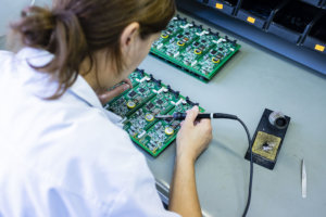
Contractual assembly of electronics (SMD, SMT, THT assembly) is the main and basic business profile of the BORNICO company. The SMD component assembly process allows placing a wide range of components on PCBs, in a variety of technologies and configurations.

In addition to the assembly of SMD and THT electronic components, we offer our clients a wide range of complementary services, which include:
-
-
- full, comprehensive logistics service – selection and supply of electronic components and printed circuits, maintaining inventory for subsequent production,
-
-
-
- testing of assembled systems – AOI 3D, visual assessment,
- functional tests with programming, additional tests and/or calibrations at the client’s request,
- washing boards in the washer using ionic purity test,
- applying protective coatings (selective painting),
- production of cables, cable bundles, bands with wires,
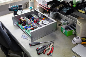
- preparation of casings (punching, drilling, cutting) and assembly of electronic components in them,
- production of finished OEM devices,
- labelling,
- technical advice at every stage of production provided by experienced electronic engineers
- Research & Development engineers
- packing and transport by courier chosen by the customer
-

Production is carried out in accordance with requirements of the IPC-A-610D standard under ESD conditions.
Inquiries for contractual assembly
We consider each inquiry individually.
To make a calculation for each offer, we need a complete BOM and technical drawing (or gerberas).
We are able to present the price offer for SMD and THT assembly (elements entrusted by the Customer) within 24 hours (business days).
We make a price offer for assembly together with completion of elements up to 10 business days.
INFORMATION REGARDING INQUIRIES SMD/THT assembly:
TECHNOLOGICAL POSSIBILITIES OF SMD ASSEMBLY
Technology
-
-
- ROHS
- PB
-
PCB size
-
-
- 50 mm x 50 mm
- panel size 360 mm x 420mm
-
The minimum size applies to the automatic assembly line. We mount smaller circuits on the another automatic machine in the off-line mode.
The minimum and maximum size of SMD components:
Range of laid elements:
-
-
- 0201 – SOP, SOJ, PLCC 45 mm, square (1.77″)
- 6 mm – QFP 20mm B(0.78″ with the raster up to 0.4mm (16 mils)
- 20 mm – QFP 45mm B(1.77″ with the raster up to 0.5mm (20 mils)
- BGA, μBGA, CSP with the regular pin distribution, minimum ball size 0.3 mm (12 mils)
-
The minimum and maximum thickness of the printed circuit:
-
-
- 0.4 mm – max. 4 mm
-
The maximum weight of the SMD component:
-
-
- max 20 grams
-
The maximum height of the SMD component:
-
-
- 15 mm
-
QUOTE FOR SMD/THT ASSEMBLY
The quote of the assembly service for each order is made individually and can be presented within: 24 hours (business days).
The quote of the assembly service together with the completion of components can be presented within: 10 business days.
Information for the quote should include:
-
-
- order quantity – number of pieces,
- component list – BOM in the xls format – containing number, component values, enclosure type, component quantity
- information regarding the side of the board on which elements are located,
- assembly drawing, or the illustrative photo,
- specific assembly requirements.
-
If the offer is to include the purchase of components, BOM should also include the catalogue designation and name of the manufacturer or the exact specification of the component including:
-
-
- working temperature ranges
- tolerance,
- enclosure type,
- temperature coefficients,
- capacitor voltages
- critical dimensions.
-
Gerber files are required for the offer for PCB printing.
REQUIREMENTS FOR PRODUCTION PREPARATION:
In the case of elements that will not have additional information, we choose them according to our own knowledge. All components selected by us will be presented to the customer for acceptance.
COMPONENTS:
If the production is made of components supplied by the customer, components should be sent in their original packaging (bulk delivery of components or components in tapes of several centimetres are unacceptable). RLC components must be delivered in tapes with the “tape leader”, min. 50 mm tape without components + 200 mm of foil.
Integrated circuits and other “large” components intended for SMD assembly should be delivered in manufacturer packaging, such as rails, trays or tapes and reels – preferably the tape. Polarized components should, in a single package, keep the same orientation. Soldering tips of components must not be oxidized or bent.
Due to enclosure defects, improper co-packing, automatic machines reject some components. Missing tips, chipped edges and non-sticked elements are the most often causes. Therefore, the customer need to provide the right amount of components with 5% of the reserve for small housings – but not less than 20 pcs. For larger housings, the reserve should be 3-5 pcs.
We return unused components to the customer.
Delivered components should be clearly described on the packaging, in accordance with the name that appears in the BOM.
Proper preparation of components delivered to BORNICO by customers will allow to meet deadlines and price conditions contained in offers prepared by our company.
Assembly drawings– pdf files – the layout scheme of components on PCB, outlines of components with numbers (required), outlines of components with values. We can also prepare the documentation based on PCB design (we will most willingly accept data in Altium, Protel, Eagle formats), and if the design cannot be delivered – based on Gerber files of the ordered design (with layers of value descriptions, numbers, board contours, reference points).
Specification of the PCB material – the order must have a specification regarding the required printed circuit board material. These are: the material type (typically FR-4), thickness (e.g. 1.55 mm), number of layers, final copper thickness, types of additional layers (solder masks, descriptive layers, tear-off masks, etc.)
REQUIREMENTS FOR THE PCB DESIGN
Fiducials – PCB design with SMD components must contain optical fiducial points (eng. fiducial). For example, it can be a round point with a diameter of 2 mm with an additional exposed 4 mm diameter solder mask. Other patterns are permissible. It should be located within each the board (not on the technological margin). For elements with a very dense raster, local smaller fiducials in the number of 2 pcs. near the corners are also helpful. The fiducial pad should also be in the paste file. Fiducials should not be covered with solder, but an automatic printer requires marking (engraving) them on the paste application template (stencil).
Packeting – optimization of assembly speed requires that small boards be delivered in panels consisting of several to several dozen boards. The optimal panel size should be within 290 x 240 mm. The packet should have 5 mm technological margins around or at least on the long sides. In exceptional cases, no margins are allowed if there are no elements in the area over 5 mm from the edge. For small boards that are over and over scoring lined, the maximum width should be smaller so that the packet is not too flaccid. The same applies to boards with small thicknesses. Individual boards should be stored in the packet without additional space. Copper layers should be separated from edges of the board by a minimum of 10 mils, so as not to damage copper during their making and separation.
Preferably, the packeting is determined by BORNICO.
Resulting files – the default format for ordering PCBs is RS-274X extended gerber.
The required layers are the minimum: copper layers, solder masks, PCB contours, paste layer (for SMT). In addition, drill files in Excellon format. For automatic assembly, pick & place files are also needed. These are text files with the position coordinates of components. Each line contains parameters of the single component. The component description must include:
-
-
- Component identifier e.g. R1,
- Value or name e.g. 1K-1%,
- Enclosure type e.g. 1206, SOT23
- Coordinates of the component center given in millimetres or inches (mils)
- Rotation angle in degrees e.g. 0
- The side for assembly: T-top, B-bottom
-
Coordinates are referenced to the origin point, the most preferably in the lower left corner. The file must also contain coordinates for the reference points – fiducials. If the design contains elements protruding beyond the outline of PCB after final assembly, such information must be included in the design, e.g. by placing outlines in gerber files. Then, during further through-hole assembly, it is possible to mount them in whole packets.
Bornico uses the Altium Designer software. Source files can be helpful in resolving some doubts. However, gerber files generated by the customer are considered as production files.
Stencil – for automatic SMD assembly, we must have solder paste applied to PCB. A sheet metal screen – stencil – is used for this purpose. It must match the panel of mounted boards and match the silk-screen printer used. Therefore, it is not possible to adapt another stencil entrusted by the customer. Bornico is responsible for the order of the stencil according to requirements. The assembly technique with SMT wave soldering in turn requires applying the glue by the stencil and components must be glued before soldering.
Double-sided SMT assembly – double-sided SMT assembly does not require usually special additional procedures. Boards go through the production process twice. Through-hole components are then soldered manually.
Other notices
Component descriptions should not overlap soldering points. If this is the case, they are usually deleted when PCB manufacturer processes files. The design should contain the visible name of the board and the current version (revision) for easy identification of the circuit.
The hole diameters given in the design refer to their final diameter (after metallization).
In the case of further assembly with wave soldering, it may be necessary to add a peelable mask that will protect the desired openings from flooding with solder.
Regarding the technique of designing standard printed circuits with SMD and THT components, we can arrange them due to increasing complications and cost of assembly:
-
-
- PCB mounted in the SMT technique (without through-hole elements), also soldered on both sides.
- the SMT board with through-hole components (THT) on the same side (can be wave soldered)
- the SMT board with through-hole components (THT) on the opposite side – wave SMT soldering after prior gluing them – applies to SMD components that can be soldered in this way.
- manual THT soldering
- double-sided THT soldering (partly wave, partly manual)
-